
role of the substrate in RF PCBs
The substrate in Radio Frequency (RF) Printed Circuit Boards (PCBs) plays a pivotal role in determining the overall performance, reliability, and efficiency of RF systems. In RF circuits, where high-frequency signals are transmitted and processed, the properties of the substrate material are critical to minimizing signal loss, maintaining signal integrity, and ensuring the stability of the circuit. The substrate serves as the foundation upon which the circuit traces, components, and other elements are mounted, and its properties directly influence how RF signals behave as they travel through the PCB.
The primary function of the substrate in RF PCBs is to provide mechanical support and structural integrity to the entire PCB. It holds the copper traces and other components in place, allowing for proper routing and connection of signals. However, its role extends far beyond simple structural support. The choice of substrate material affects the electrical characteristics of the PCB, particularly the signal propagation speed and loss, making it a critical factor in the design of high-frequency circuits.
One of the most important properties of the substrate is its dielectric constant (also known as relative permittivity). The dielectric constant of the substrate material affects the speed at which signals travel along the PCB traces. RF signals propagate more slowly in materials with a high dielectric constant, which can introduce delays and affect the timing of signal transmission. For high-frequency applications, such as wireless communications and radar, it is important to use substrates with a lower dielectric constant to ensure that signals can propagate efficiently and with minimal delay. Common substrates with lower dielectric constants include materials such as PTFE (Polytetrafluoroethylene) and ceramic-filled epoxies, which are ideal for high-speed RF circuits.
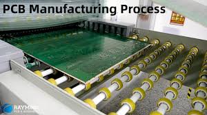
What is the role of the substrate in RF PCBs?
Another crucial factor influenced by the substrate is signal loss or attenuation. As RF signals travel through the PCB traces, some of the signal energy is lost due to the resistance of the substrate material, a phenomenon known as dielectric loss. Substrates with high dielectric loss contribute to greater signal attenuation, reducing the strength of the signal as it travels. This can result in poor signal quality, decreased range, and even failure to meet the required communication standards. To minimize signal loss, rf pcb are often made with low-loss substrate materials that help preserve the integrity of the high-frequency signals. Materials like PTFE, for instance, are often used in RF applications because they offer low dielectric loss and are highly effective at minimizing attenuation.
Thermal management is another important role of the substrate in RF PCBs. High-frequency circuits often generate significant amounts of heat, especially in power amplifiers and other active components. The substrate material must have good thermal conductivity to dissipate heat effectively, preventing overheating and ensuring that the circuit operates within its optimal temperature range. Substrates with poor thermal conductivity can lead to the accumulation of heat, which can damage sensitive components and negatively affect the performance of the RF system. Materials like ceramic and certain composite substrates are often chosen for their excellent thermal properties, helping to ensure long-term reliability and stability in RF applications.
In addition to its electrical and thermal properties, the substrate also plays a role in impedance control in RF PCBs. Impedance matching is crucial for minimizing signal reflection and ensuring that the signal is transmitted efficiently across the PCB. The substrate material influences the impedance of the traces, as the distance between the trace and the ground plane, as well as the trace width, are both affected by the substrate’s dielectric properties. A consistent and controlled impedance is essential for ensuring high-quality signal transmission and minimizing losses or distortions. Designers carefully select the substrate material to match the required impedance characteristics of the circuit, ensuring that the RF signals are transmitted with minimal reflection and optimal efficiency.
Finally, the substrate also impacts the cost and manufacturability of RF PCBs. While high-performance substrates, such as PTFE and ceramics, provide excellent electrical properties, they are often more expensive and challenging to fabricate compared to traditional FR4 materials. Therefore, designers must balance performance requirements with manufacturing constraints and budget considerations. In some cases, a combination of different substrate materials may be used to optimize both performance and cost.


